Sản phẩm đã cho vào giỏ hàng
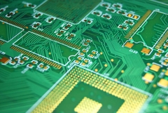
1. Cutting: Cut the initial copper clad laminate into plates.
2. Drilling: Drill the hole diameter at the corresponding position on the sheet according to the material.
3. PTH: A thin layer of copper is deposited on the insulating hole wall by chemical method.
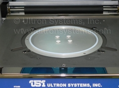
4. Exposure: Transfer the image on the production film to the board.
5. Plating: Let the hole and circuit copper layer be plated to a certain thickness (20-25um), and finally meet the requirements of the finished copper thickness of the final PCB board.
6. Film stripping: Use NaOH solution to expose the non line copper layer of the anti plating coating.
7. Etching: Corrode the copper layer of non line parts by chemical reaction method.
8. Soldermask: Transferring the green film pattern to the board can protect the circuit and prevent tin on the circuit when welding parts.
9. Silk screen and cure: Print the required text and information on the board.
10. Surface finish: Because bare copper is susceptible to moisture and oxidation if exposed to the air for a long time, surface treatment should be carried out. Generally, common surface treatments include tin spraying, gold precipitation, OSP, tin precipitation, silver precipitation, nickel palladium, electric hard gold, electric gold fingers, etc.
11. Profiling: Let the PCB be cut into the required overall dimensions by CNC molding machine.
12. Testing: Check the status of the analog board to see if there are defects such as short circuit.
13. Final inspection: Inspect the appearance, size, hole diameter, plate thickness, mark, etc. of the plate